
Printed circuit boards (PCBs) have transformed the world of electronic manufacturing. Today, millions of devices, from smartphones to laptops, gaming consoles, appliances, and industrial machines, use PCBs to connect complex components and facilitate electricity flow. In other words, they set the foundation for electronics to function per their design. However, due to practically unlimited variations in design and components, custom PCB ordering has become an essential aspect of manufacturing and fabrication.
In other words, when electronics companies order PCB boards, they tailor the design and specifications according to their products and components. Hence, you need to understand what advanced PCB manufacturing and fabrication entails.
In this post, we’ll share a brief overview of the process. So, if you’re looking to order circuit board for your electronic device, you know what to expect and look for in terms of design, quality, and cost.
PCB Structure, Components, and Types
Before diving into PCB manufacturing and fabrication, you must understand the basic structure of a printed circuit board and the essential components that work together to enable its functionality:
Structure
When you order PCB boards, here’s what you can expect to find in terms of layout, components, and structure:
- Substrate – All PCBs comprise a substrate made from fiberglass or other rigid materials. It serves as the circuit board’s base to rest all the essential components.
- Copper Layers – Next, you can find thin layers of copper foil sandwiched onto the substrate. These layers set the foundation for electrical conductivity by enabling current flow between components.
- Solder Mask – Copper is incredibly prone to oxidation, which can lead to solder bridging and other issues. Hence, the solder mask is a protective shield to optimize the circuit’s structural integrity and keep the connections in place.
- Silkscreen – As mentioned earlier, PCB ordering is a large-scale process, with over a hundred million boards produced annually on average. Therefore, PCB manufacturers must proactively distinguish designs and components to aid technicians and fabricators. This is where the silkscreen comes in. It contains essential information and markings to simplify identification and assembly.
Essential Components
Below are the key components of a printed circuit board:
- Active and Passive Electronic Components – Common electronic components include transistors, microcontrollers, capacitors, resistors, etc. You can find a wide selection of these components at Kunkune Electronic Component Store, known for its dedication to customer satisfaction and commitment to excellence in every product offered.
- Conductors – All PCBs consist of interconnecting conductors that create pathways for consistent electricity flow in the circuit. Common examples include copper traces and vias.
- Pads and Landings – Pads are copper-plated areas on a PCB where engineers rest and solder circuit components. Similarly, landings are found beneath the surface where vias connect to the component pads.
- Mounting Holes and Edge Connectors: Printed circuit boards feature holes to secure the electronic device’s chassis or enclosure structure. In contrast, edge connectors are metal contacts used to connect flex PCBs or external devices.
- Testing Points – Since PCBs are prone to performance fluctuations and failure, manufacturers add accessible testing points for technicians to test functionality or troubleshoot issues during component assembly and post-purchase checkups.
What Happens When You Order PCB Boards? A Step-by-Step Walkthrough of PCB Ordering, Manufacturing, and Fabrication
PCB ordering is a complex and strategic manufacturing process. Each step requires proactive planning and precision to achieve the desired functionality and quality of the final product. Hence, industries that order circuit board, including automotive, consumer electronics, healthcare, and aerospace, provide specific requirements and standards for PCB manufacturers to meet.
Below is a step-by-step overview of the process, from the initial brief to shipping:
1. Brief and Requirements Gathering
In the first step, PCB manufacturers gather all the project details and requirements from clients, including:
- Design
- Specifications
- Type
- Functionality
- Performance expectations
- Quantity
- Timeline, etc.
With this comprehensive brief, they create a customized roadmap and outline each milestone from design to delivery.
2. Schematic Capture
Next, engineers create a schematic capture of the printed circuit board based on the client’s requirements. The digital diagram simply serves as the PCB’s blueprint, virtually displaying the complex connections in the circuit and each component’s functionality.
The process involves using advanced EDA software like Cadence Allegro or Altium Designer to design the circuit layout and strategically select and place components from digital libraries to establish the circuit’s logic and ensure proper electricity flow and distribution.
During the process, manufacturers must adhere to industry standards and best practices to ensure the end product is functional, reliable, and durable. Popular bodies include:
- ISO 9001 – Quality Management Systems Standard (relevant for PCB manufacturing)
- IPC-4101 – Specification for Base Materials for Rigid and Multilayer Printed Boards
- IPC (Association Connecting Electronics Industries)
- UL 796 – Standard for Printed-Wiring Boards
- IPC-A-600 – Acceptability of Printed Boards
- IEC 61191 – Printed board assemblies
- IPC-6012 – Qualification and Performance Specification for Rigid Printed Boards
- IPC-6013 – Qualification and Performance Specification for Flexible Printed Boards
- IPC-2223 – Sectional Design Standard for Flexible/Rigid-Flexible Printed Boards
- ANSI/IPC-2221A – Generic Standard on Printed Board Design
3. Routing and Tracing Simulation
Once the digital circuit board is ready, engineers run routing and tracing simulation tests by analyzing the electrical signals and ensuring they follow the intended routes without interference or cross-talk. These tests aim to identify and eliminate issues like impedance mismatches or signal distortion to maximize the final product’s performance, reliability, and integrity.
4. Prototyping and Testing
Prototyping and testing are the most critical stages in PCB manufacturing and fabrication. It involves producing a small batch of PCBs based on the final design and simulation then assembling and soldering them together. The prototype undergoes rigorous testing, including functional testing to verify its performance according to specifications, electrical testing to measure voltage, current, and impedance, and environmental testing to assess its durability under different conditions. Any issues or deficiencies discovered during testing are addressed, and the design may be revised before mass production begins.
5. Component Procurement
Just like clients who order PCB board, manufacturers procure all the necessary parts for PCB assembly from various suppliers, including (but not limited to):
- Inductors
- Diodes
- Resistors
- Integrated circuits
- Capacitors
- Transformers, etc.
During the procurement process, they consider various factors to ensure they get quality parts at the right price. Once they’ve identified the suppliers, they place orders and await delivery. As straightforward as this process may sound, it requires strategic planning to ensure all the necessary parts are available before assembly. So, it’s like putting together a puzzle, but instead of finding the right pieces, you’re finding the right components for our PCBs.
6. PCB Fabrication
Now, we’ve reached the business end of the PCB ordering process in which large-scale production begins. Engineers use the tried-and-tested prototype to mass produce the final product. The process typically starts with a blank copper-clad board. Then, the technicians add a layer of photosensitive material called “resist” to the board. Once done, the board undergoes photolithography – a process that uses high-intensity UV light to fabricate thin-film patterns on the board. However, it often results in copper traces on the circuit surface. Fortunately, they can be etched away with a quick chemical bath. Finally, the manufacturer coats the board with a protective layer to prevent corrosion and damage.
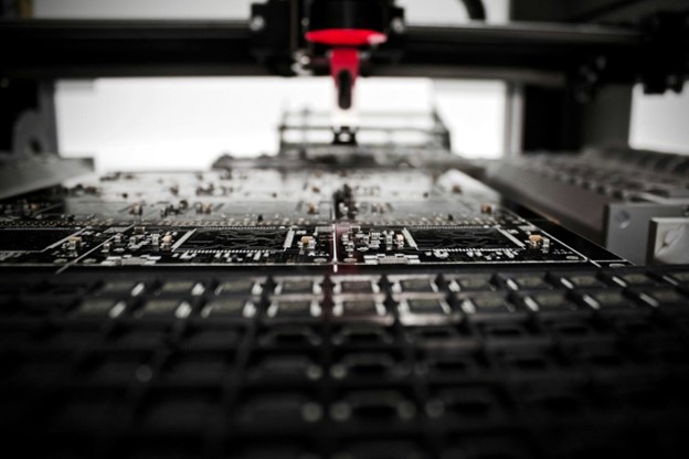
7. Assembly and Soldering
Following the fabrication stage, the PCB is assembled like a puzzle with tiny electronic parts. First, the technicians place the components on the board using pick-and-place machines or by hand before applying solder paste to the boards’ pads. Once ready, the entire assembly goes through a reflow oven, where the solder paste melts, and the components are permanently attached to the board. After that, any excess solder is cleaned off, and the PCB is inspected for defects.
8. Quality Control
Once the assembly process is complete, each board undergoes rigorous testing to identify defects or issues. This includes functional testing to verify that all components are working correctly and that the PCB performs as expected. Visual inspection also checks for any physical defects or soldering errors. Any boards that fail to meet our quality standards are returned for rework or repair. By maintaining strict quality control measures, manufacturers ensure customers receive only the best-quality PCBs.
9. Packaging and Shipping
Finally, once the PCBs have passed quality control and testing, they’re carefully packaged for protection during transit with anti-static bags/foams to prevent damage from static electricity or physical impact. The packaged boards are then placed in sturdy boxes with appropriate padding to ensure their safety further. Once packaged, the PCBs are ready for shipping to our customers. Most manufacturers proactively partner with reliable shipping carriers to ensure timely delivery with minimal damage.
PCB Ordering, Manufacturing, and Fabrication – Conclusion
In a nutshell, the PCB ordering process covers various stages, from design to delivery. By understanding the nuances of PCB manufacturing and fabrication, customers can ensure they receive high-quality boards tailored to their needs. From the moment you order PCB board to receiving the final product, each stage requires attention to detail and collaboration between manufacturers and customers.